The Internet of Things is an amalgamation of technology and matter to provide faster solutions to day-to-day problems. Apart from a PC, many devices use this mix of physical and digital components that make the digitalized life easier for the end-user. One of the most prominent examples of an IoT is a smartphone. In recent times, due to multiple technological as well as digital advancements, apps have become an inevitable part of our daily lives. Modern apps with the ability to control home utilities and appliances, the emergence of vehicles enabled with data accessibility, and tech as attire Bluetooth earphones are extending the limits of IoT every second.
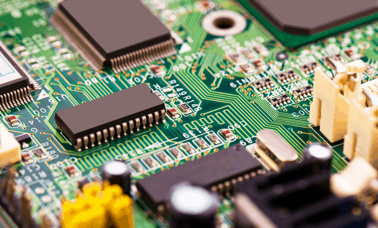
Printed circuit board (PCB) designing is an intrinsic mechanism that enables expansion of the Internet of Things. The primary role of PCB is to enliven the electronic circuits in tangible form. The process entails PCB layout service. The combination of various components placed appropriately and directional routing is the basis of PCB board design. This is done to establish electrical connectivity on an electrically constructed circuit board.
The interplay of PCB designing and IoT results in the smooth functioning of various devices. PCB designing is an influencer for fostering efficiency in IoT.
The essential areas where PCB designing plays a vital role in advancing IoT are:
- Size: The majority of IoT devices are tiny in size. The required components are also demanded in small sizes. An example would be, MEMS technology used in the creation of modern sensors. This process is cheap and durable as well as provides a small footprint. Due to the dearth of space availability, a PCB layout engineer has minimal scope for board layout. The main challenge for him is to place the essential components such as vias, track placement, and other relevant technical pieces. The advancement in the IoT industry is demanding that PCB designers come up with swift and flexible solutions. Flex boards along with high-density interconnects are becoming high in demand. Such technical advancement would increase the overall effectiveness and productivity of the IoT industry. Constant research and development in PBC have been finding improvised solutions to make IoT a faster-growing sector. More functionality in less available space is the trick here!
- Power: There is continuous communication of IoT devices with their various networks. This phenomenon takes a toll on the power consumption of IoT devices. As a result, the general focus of the PCB designing department is on coming up with ways to increase the battery life and the integrity of available power. The requirement of selecting a good power management system to optimize power becomes a task of paramount importance for PCB designers. Choosing ICs that fit within the budget framework of a circuit’s functional blocks becomes crucial. The battery life of IoTs depends on power consumption. Designers need to keep in mind the operating conditions and various states of the device. IoTs with wireless transceivers exhibit varying frequencies at alternating transitions. Subsequent power support is required for a better battery life.
- PCB Layout: The spaces available for routing traces are extremely limited in IoT devices. Given such scenarios, Multilayer PCBs remain the best choice for IoT gadgets. The inherent components are of high density demanding interconnects of equivalent density. As a result, the designers reduced the pad sizes and enhanced the total number of vias. The PCB design is a byproduct of market requirements. There is no absolute autonomy as several factors guide their design such as:
- Device application environment
- Component placement
- Flexibility
- Layout, 2D or 3D
- Rigid-flex circuits enabling flex routing
- Form fills
- Flex layers
- PCB Material: With the growing popularity of IoTs certain materials have grown in demand as well. HDI PCBs and flex remain the two elementary innovative materials to have gained increased popularity. The demand for smaller-sized components is increasing with the ever-specified requirements of various IoT devices. The flexibility of PCBs and the interconnect of high density have given rise to the trend of PCB materials. Flexible PCBs demonstrate impressive strength during mechanical turbulences. An additional benefit is the simplicity of their circuit wiring. Furthermore, in a smaller space, more components can be fit.
- Thermal Adjustment: Managing the thermal arrangement is a crucial factor in IoT devices. As a consequence, PCB engineering needs to observe the balancing of hotspot formation. Using copper planes and copper-plated thermal vias will enable heat dissipation. The intrinsic requirements that demand thermal adjustment are battery power, small size, and case enclosures without slots. A holistic grounding will help heat dissipation as well as RF connectivity.
In terms of US dollars, During the forecasted period of 2021 to 2026 the Compound Annual Growth Rate is projected to be 16.7 %. The IoT products cover a wide array of products such as tech wearables, smartphones, smart watches, automated home appliances, connected cars, rings, smart thermostats, and many others. The industry is on the rise and constant research and development can bring about new additions to the product list.
Last Words
IoT represents the arrival of a new age of living. The power of automation is escalating towards its zenith and IoT is the industry that stands as a testament to this phenomenon. A crucial counterpart of the IoT industry is PCB designing. It is the interactivity of IoT and PCB that is revolutionizing modern-day living. With multiple products emerging in the market. The role of PCB is becoming an ever-challenging one for the designers and the engineers. One of the key roles played by PCB is incorporating design technology in embedded systems. This process entails designers from hardware as well as firmware getting together for a common purpose. It is to create embedded systems from the very scratch.
The relationship between IoT and PCB is like a marriage. Where PCB operates continuously to make the IoT look good in the market. It is an interlinked relation that is amazing to the consumer base constantly. IoT keeps on throwing challenges at the PCB industry constantly. The basic reason for this is the technological advancements that are guiding market forces. The combination of both industries is bringing about a landscape-changing revolution in the technological industry. This is just the beginning. The coming years may see many more groundbreaking byproducts of this marriage!